SERVICE
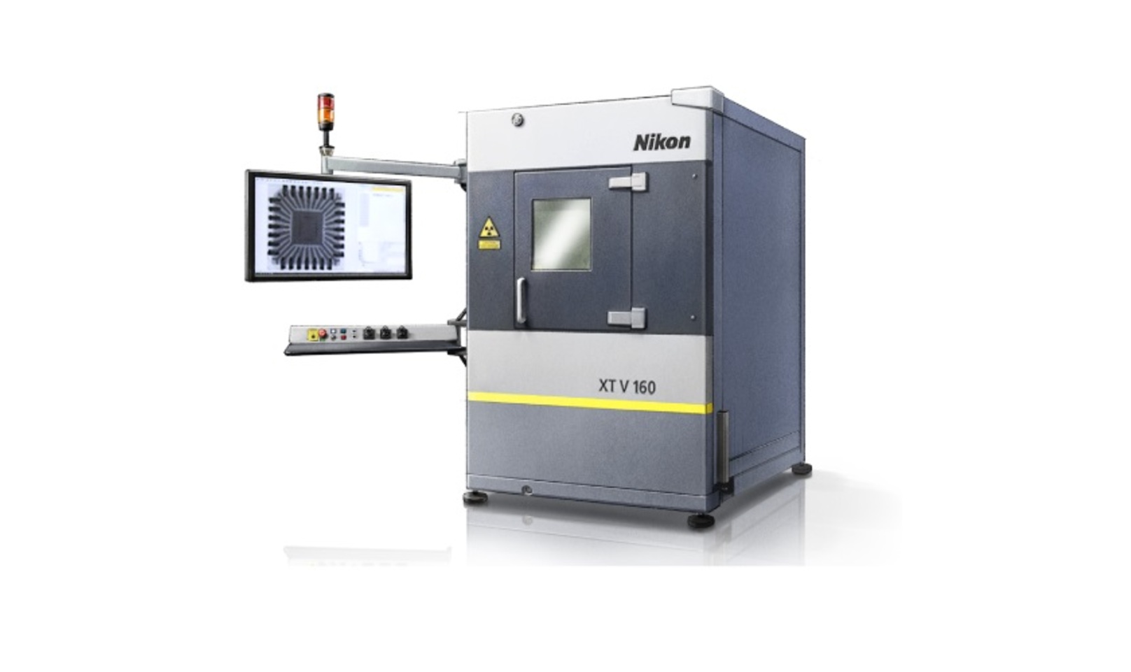
XT V Series: The Ultimate Solution for Electronic Components and Semiconductor Inspection
Product Info
The XT V 130C and XT V 160 are X-ray inspection systems designed for precise non-destructive testing of electronic components and semiconductors. These systems meet stringent quality requirements, such as lead-free solder quality assurance, defect detection in components, and BGA (Ball Grid Array) inspection. NIKON SALES (THAILAND) CO., LTD. proudly delivers this advanced technology from the Nikon Group to businesses in Thailand.
■ Key Features
・High Resolution
XT V 130C: Supports feature recognition at 2 μm
XT V 160: Supports submicron-level feature recognition (500 nm)
・Multi-Axis Control
XT V 130C: 4-axis control (X, Y, Z, tilt)
XT V 160: 5-axis control (X, Y, Z, tilt, rotation) for comprehensive inspection capabilities
・Smooth and Intuitive Operation
Equipped with Inspect-X software and joystick controls, enabling real-time and seamless inspections.
・Cost-Effective Operation
Open tube design ensures low running costs and long service life.
・Safety-Oriented Design
Complies with DIN 54113 radiation safety standards, with a lead-lined cabinet for complete protection.
■ Specifications
・Maximum Energy:
XT V 130C: 130 kV / 10 W
XT V 160: 160 kV / 20 W
・Maximum Geometric Magnification: 2,046x
・Maximum Sample Size: 711 mm × 762 mm
・Maximum Weight: Supports up to 5 kg
・Imaging System: 16-bit flat panel detector
■ Applications
・Electronic Component Inspection
Detecting defects in BGA, QFN, QFP, and wire bonding
・Semiconductor Inspection
Quality assurance for flip chips, micro bumps, and TSV (Through Silicon Via)
・Mass Production Inspection for Small Parts
Serial inspection of cables, LEDs, and plastic components
XT V Series supports high-precision non-destructive inspections required in manufacturing plants and research facilities, enabling productivity enhancement and cost savings.
For More Information Please download the PDF or contact us for further details.
CONTACT

